
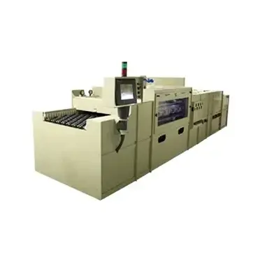
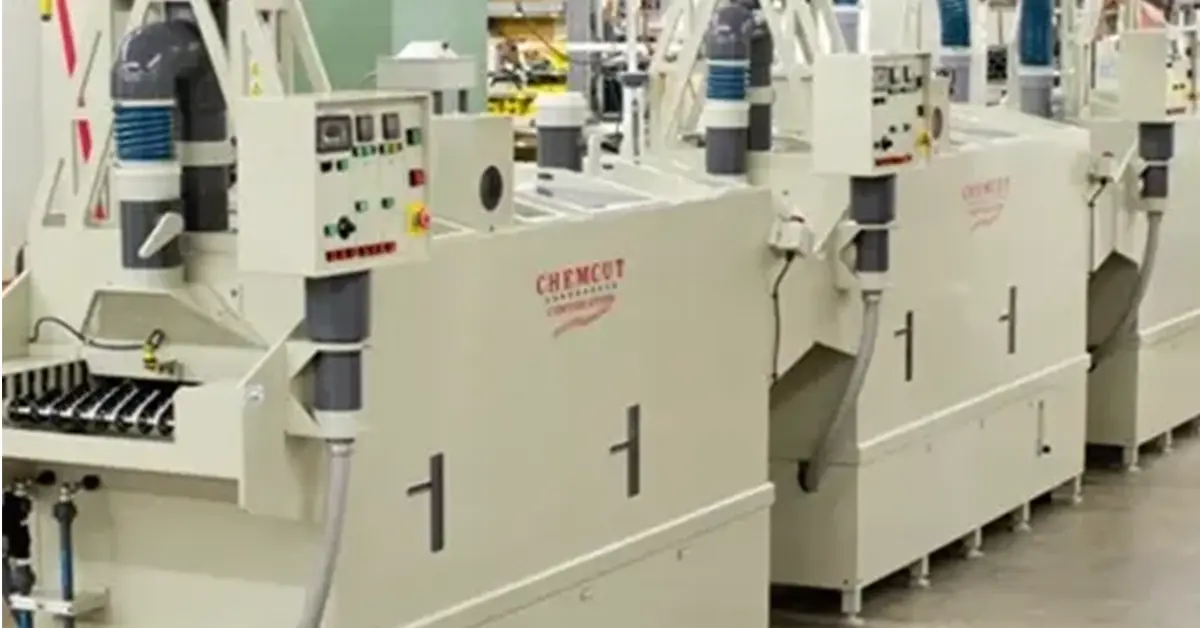
XLi Developing Systems
Available Conveyor Widths
- 20″
- 30″
- 40″
- 50″
- 60″
Common Processes
- Custom Size (1 to as many chambers as you want)
- Developer (Stand Alone)
- DES (Develop – Etch – Strip)
Common Chemicals
- 1% Potassium Carbonate
- 1% Sodium Carbonate
2300 Series Developing System
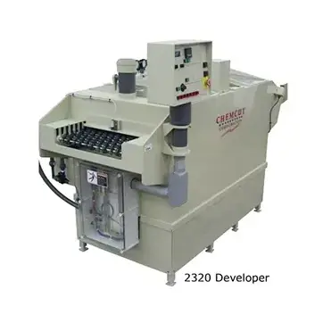
Available Conveyor Widths
- 15″
- 20″
- 30″
Common Processes
- Custom Size (1 to as many chambers as you want)
- Developer (Stand Alone)
- DES (Develop – Etch – Strip)
Common Chemicals
- 1% Potassium Carbonate
- 1% Sodium Carbonate
Common Resists
- dry film photoresists
- liquid photoresists
- Aqueous solder mask resist (dry and liquid)
- And many more resists
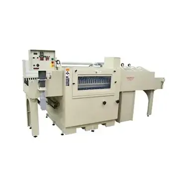
CC8000 Developing Systems
Available Conveyor Widths
- 20″
- 30″
- 40″
- 50″
- 60″
Common Processes
- Custom Size (1 to as many chambers as you want)
- Developer (Stand Alone)
- DES (Develop – Etch – Strip)
Common Chemicals
- 1% Potassium Carbonate
- 1% Sodium Carbonate
Common Resists
- dry film photoresists
- liquid photoresists
- Aqueous solder mask resist (dry and liquid)
- And many more resists

How to Scale Up Production with Chemical Milling & Etching
Chemical milling and etching are powerful techniques widely used in industries requiring precise,...
11 Things Needed to Start a Chemical Etching Plant | Chemcut Blog
11 Things You Need to Start a Chemical Etching Plant Chemical etching has been around since 2500...
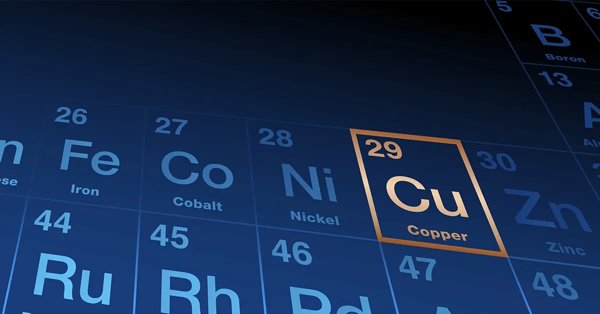
Copper Etchant Options | ChemCut
Copper etching is a vital manufacturing process that tends to be used in the manufacturing of...