Photoresist Developers for High Resolution
Product Lines for Photoresist Developers
We offer multiple photoresist developer product lines, all of which can be easily customized to accommodate your unique process. Review the options, then speak with one of our experts about developing the custom solution you need.

XLi Developing Systems
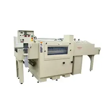
- 20″
- 30″
- 40″
- 50″
- 60″
- Custom Size (1 to as many chambers as you want)
- Developer (Stand Alone)
- DES (Develop – Etch – Strip)
- 1% Potassium Carbonate
- 1% Sodium Carbonate
2300 Series Developing System
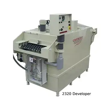
- 15″
- 20″
- 30″
- Custom Size (1 to as many chambers as you want)
- Developer (Stand Alone)
- DES (Develop – Etch – Strip)
- 1% Potassium Carbonate
- 1% Sodium Carbonate
- dry film photoresists
- liquid photoresists
- Aqueous solder mask resist (dry and liquid)
- And many more resists
CC8000 Developing Systems
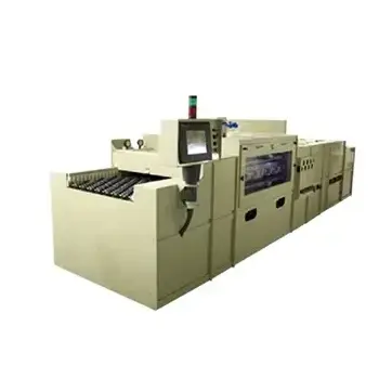
- 20″
- 30″
- 40″
- 50″
- 60″
- Custom Size (1 to as many chambers as you want)
- Developer (Stand Alone)
- DES (Develop – Etch – Strip)
- 1% Potassium Carbonate
- 1% Sodium Carbonate
- dry film photoresists
- liquid photoresists
- Aqueous solder mask resist (dry and liquid)
- And many more resists
Important Pre-Developing Steps
Alkaline and Acid Clean—Chemcut Processes
- Cleaning the metal surface is extremely important when it comes to developing. A clean surface means no dirt will interfere with the exposure step, and lamination adhesion is improved.
- Alkaline Clean is the first cleaning step and is used to remove all oils and organics from the surface.
- Acid Clean is the second cleaning step and removes any contaminants that remain on the surface. This chemistry will micro-etch the surface, which increases lamination adhesion.
- To further increase lamination adhesion, chemical milling companies should make their post-acid clean rinses slightly acidic. A slightly acidic rinse will create an acid surface that reacts with the lamination to improve adhesion.
- PCB industry companies can Increase lamination adhesion by micro-etching the surface prior to lamination.
Lamination—Non-Chemcut Process
- Hot Roll Lamination— pre-heating the board before applying the dry film photoresist—is used to increase resist adhesion and avoid photo resist wrinkling, especially if the metal is thick.
- Liquid Resist is recommended to attain high resolution for developing and etching.
- Thinner Photoresist typically gives tighter tolerances because the channel the chemistry needs to enter is shorter. A shorter channel allows the chemistry to flow in and out better.
- Hold for 30 minutes after lamination to allow the resist to lock into the metal.
Exposure—Non-Chemcut Process
- As products continue to get smaller this has become one of the most important pre-developing steps.
- A speck of dirt is enough to cause an open circuit on fine lines. The slightest misalignment on artwork top to bottom has the potential to shift dimensions outside the tolerances.
- This is not a Chemcut process, but over the past seven decades, we have learned a lot about photoresist exposure. Below is a small list of topics we believe are important for the best exposure:
- Clean
- Yellow room is a must have
- Collimated light for fine features
- Features that help create near perfect alignment
- Hold for 30 minutes before developing for better resolution
Developing Step
- Developing is often viewed as less critical than etching. While that may be true, it does not mean you can overlook the developing step.
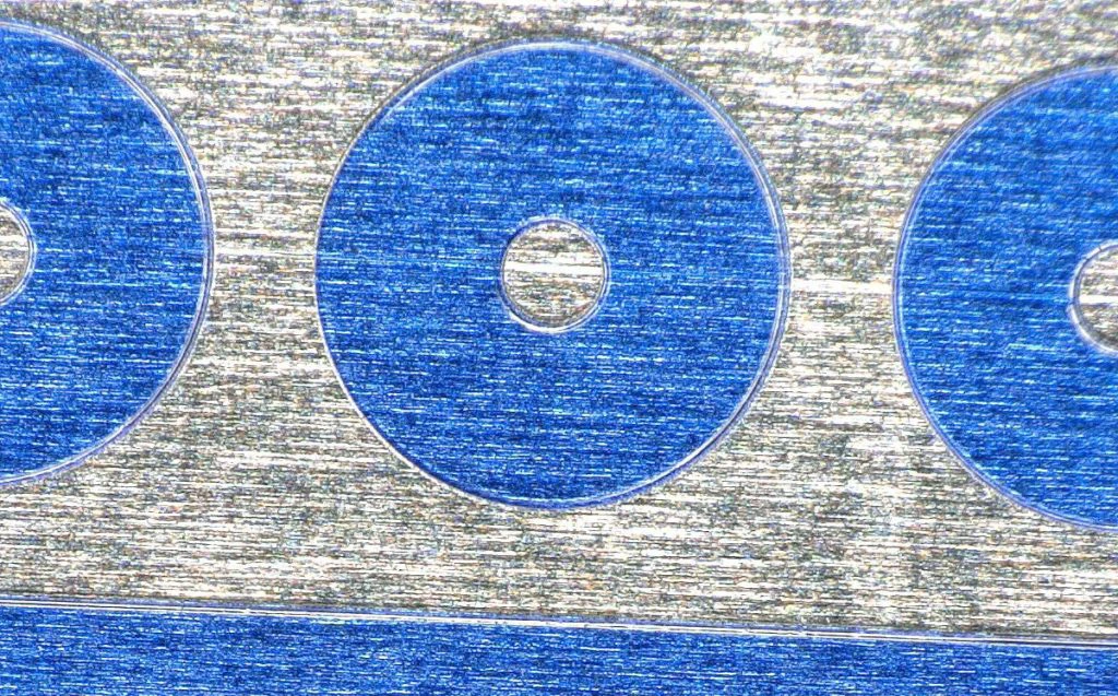
- Photoresist can be underdeveloped or overdeveloped. Underdeveloped means all the unpolymerized resist was not completely removed. You did not fully expose the metal that you want to etch away, resulting in smaller holes, no breakthrough for chemical milling, and shorts for circuits.
- Overdeveloped means the developing solution started to undercut the resist. As a result, the resist may lift while etching, which means you will lose resolution and worse, etch away metal you want to keep. For chemical machining, you may end up outside your tolerances. For circuits, you may end up with open circuits.
Important Post-Photoresist Developing Steps
- Optional steps to increase lamination adhesion:
- Bake is the most commonly used step to increase resist adhesion. The major downfall of this step is the time it takes to complete.
- UV Bump is a much quicker step. However, it does not increase adhesion nearly as much as baking does.
-
Etch
-
Strip
Related Resources
Optimize a Wet Processing for Design & Spacing
Effective space planning and design are critical to the success of wet processing facilities....
How to Scale Up Manufacturing | Strategies to Improve Efficiency & Reduce Costs
Scaling up manufacturing presents both challenges and opportunities for engineers who must...
How to Scale Up Production with Chemical Milling & Etching
Chemical milling and etching are powerful techniques widely used in industries requiring precise,...
High quality products are made with high quality equipment. Stake your reputation on Chemcut.
Already a customer?
Chemcut’s commitment to you goes beyond the sale. We keep your equipment running with the industry’s best post-sales support, which includes our in-house R&D lab and global field service assistance.
We also maintain the industry’s largest and most diverse inventory of high-quality replacement parts to ensure prompt delivery regardless of the type or age of your Chemcut or MEI Division equipment.